Sustainable Energy
Scaling Up Solar Power
Applied Materials makes the equipment needed to produce the biggest solar panels in the world.


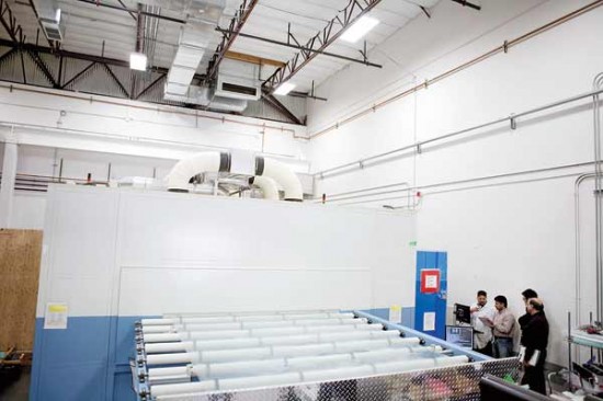
In 2006, semiconductor-equipment giant Applied Materials got into the solar-power market in a big way. At the company’s headquarters in Santa Clara, CA, you can see just how big: a ceiling-mounted crane lifts a piece of glass the size of a garage door onto a table for testing. The glass sheet, covered with a thin orange film of amorphous silicon, is destined to become one of the world’s largest solar panels.
Applied Materials developed the equipment to produce these extremely large photovoltaic panels in order to lower the price of solar power–crucial if solar is to compete on price with fossil-fuel electricity. The value of a solar installation comes down to the cost of each watt of power it can produce over the lifetime of a panel, and Applied Materials’ panels bring down costs in two ways. The equipment for manufacturing thin-film solar cells operates more efficiently when the panels are bigger. And larger modules need less hardware and labor to wire them together and support them.
Applied Materials, which was already the largest equipment supplier to the semiconductor and liquid-crystal-display industries, brought its expertise to solar power in 2006. The company’s photovoltaics and its display backplanes are both based on glass panels coated with amorphous silicon. Its production facilities were already set up to make those panels in 10 sizes, so achieving the best cost per watt was simply a matter of picking the right surface area, says Jim Cushing, senior director of the photovoltaic-equipment line. The result was “by far the fastest ramp to production in the PV industry,” he says–from lab to market in just under two years.
Applied Materials now sells a complete set of equipment for transforming large glass panels into thin-film solar cells, transporting it to manufacturers in several shipping containers. The company claims that each factory using its equipment can produce enough solar cells every year to generate 80 megawatts of power, enough to provide energy for 35,000 U.S. homes during peak hours of electricity use.
The process of building the solar panels themselves starts with glass sheets 2.2 by 2.6 meters in area and only 3.2 millimeters thick. These come to a factory precoated with a micrometer-thick film of a transparent conductive metal oxide that will serve as the top electrical contact in the finished panel. A robotic arm shaped like the business end of a forklift loads the delicate glass sheet onto the metal rollers of a conveyor belt, which moves it through a cleaner and then through a seamer that reinforces its edges to prevent chipping during manufacturing. The panel then travels through a machine called a laser scribe, which carves lines through the conductive coating to define the boundaries of each of 216 cells on the panel.
The panel is now ready to be coated with two silicon films that will absorb sunlight and convert its energy into electrical current. First is a layer of amorphous silicon, which strongly absorbs light from the blue end of the spectrum. A second robotic arm slides the panel into the airlock of an apparatus called a plasma-enhanced chemical-vapor deposition chamber. Inside, the air is pumped out; silane, a gas composed of silicon and hydrogen, is pumped in and ionized. In the resulting reaction, the gas decomposes, depositing the silicon uniformly on the glass.
Conveyer belts and robots then move each panel down the line to one of three additional vapor deposition chambers, where it is coated with a film of multicrystalline silicon. This layer absorbs red light, allowing the panels to take advantage of more of the energy in sunlight. Forming multicrystalline silicon takes time and care, but having three systems perform this step on different panels in parallel keeps it from slowing down the entire manufacturing process.
Moving down the conveyer belt, each panel goes through another laser scribe to carve the silicon films into cells whose boundaries align with the patterns in the conductive layer. The panels are then coated with three layers of metal that act as a back electrical contact; after another scribing step to shape a contact for each cell, they are nearly finished. If the manufacturer wants to cut the giant panels in half or even into four pieces, that happens at this point. Then, to ensure that a person who touches the edges of the finished panel won’t get electrocuted, the borders of the conductive areas are edged off and the glass is reseamed to fill in the space.
Next, a top piece of glass is laminated to each panel in a process similar to that used in making car windshields. Finally, a junction box for carrying electricity from the panel is added to the back. Each completed panel is exposed to a solar simulator to test its output and then marked with a performance rating.
When Applied Materials started producing equipment for making the large modules, many in the business assumed that each panel would be sliced into smaller pieces, says John Benner, manager of PV-industry partnerships at the National Renewable Energy Laboratory in Golden, CO. But the company made a good case for leaving them intact. Because of their large area, the modules have among the highest power outputs in the industry–about 500 watts. The large size leads to savings on installation costs that help the panels compete with other thin-film systems on the market. The cost of electricity generated by the giant panels is $3.50 a watt, including installation.
Panels of this size are best suited for use in massive ground-based solar farms. Several such facilities have already been built, including a 500-kilowatt farm in Neustadt, Germany, that contains thousands of modules. Seven factories equipped with the technology are up and running at full volume and have manufactured more than a million of the modules.
The next challenge Applied Materials has set itself is to bring manufacturing costs down to $1 per watt by the end of this year. Its thin-film modules will have to compete with those made by other companies that are exploring alternatives to silicon–alternatives that are expected to reduce manufacturing and materials costs even further.